SUSS MicroTec SE
SUSS MicroTec SE
Schleissheimer Str. 90
85748 Garching
Deutschland
https://www.suss.com/de
Jessica Boehler
Senior Manager Brand & Marketing Communications
Contact per mail
Profile
SUSS, founded in Munich in 1949, has helped shape the semiconductor industry since its beginnings, including the development of the world's first mask aligner in 1963. The company now offers a comprehensive portfolio of high-precision process solutions for key steps in microfabrication. Together with research institutes and industrial partners, SUSS develops innovative solutions for technologies such as 3D integration and nanoimprint.
Technology / Research
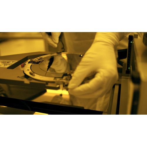
- Photomask processing
- Wafer cleaning:
- Current research focus: Development of resource-efficient, chemical-reduced cleaning processes
- Temporary and permanent wafer bonding including hybrid bonding:
- Current research focus: Development of new processes and materials to maximize bond quality in permanent and hybrid bonding
- Lithography:
- Current research focus: high-precision UV lithography
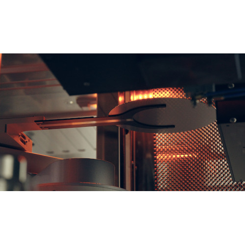
- Coating and development:
- Current research focus: integration of adaptive process strategies such as inkjet printing for flexible substrates and heterogeneous materials
Products / (services) performances
- Photomask systems:
- For Bake & Develop
- For cleaning
- Wafer cleaner
- Wafer bonder:
- Temporary bonder
- Permanent bonder
- Hybrid bonder
- Lithography solutions:
- Mask-Aligner
- UV projection scanner
- Coating systems:
- Coaters and developers
- Inkjet printers
- Metrology solutions:
- For coaters
- For bonders
- For mask aligners
- For photomasks